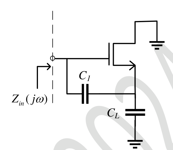
In the circuit below, assume that the long channel NMOS transistor is biased in saturation. The small signal trans-conductance of the transistor is $g_m$. Neglect body effect, channel length modulation and intrinsic device capacitances. The small signal input impedance $Z_{in}(j\omega)$ is ________.
The drain is at AC ground, so the stage is a source follower with $C_1$ between gate and source and $C_L$ from source to ground. Let $x=v_g-v_s$. The input current is $I=j\omega C_1x$ (the gate draws none). KCL at the source: $(j\omega C_1+g_m)x=j\omega C_Lv_s$. Then $v_g=x+v_s=x\,\dfrac{g_m+j\omega(C_1+C_L)}{j\omega C_L}$ and $Z_{in}=\dfrac{v_g}{I}=\dfrac{g_m+j\omega(C_1+C_L)}{-\omega^2C_1C_L}=\dfrac{-g_m}{C_1C_L\omega^2}+\dfrac1{j\omega C_1}+\dfrac1{j\omega C_L}$ (a negative resistance in series with the two capacitors).
More BJT and MOSFET Amplifiers questions
GATE 2024 EC Q18– For the closed loop amplifier circuit shown below, the magnitude of open loop low…
GATE 2024 EC Q51– In the circuit shown below, the transistors M 1 and M 2 are biased in saturation. Their…
GATE 2023 EC Q21– In the circuit shown below, V 1 and V 2 are bias voltages. Based on input and output…
GATE 2023 EC Q22– A cascade of common-source amplifiers in a unity gain feedback configuration oscillates…
GATE 2023 EC Q64– In the circuit below, the voltage V L is V (rounded off to two decimal places).
GATE 2022 EC Q18– Consider the CMOS circuit shown in the figure (substrates are connected to their…