GATE 2024 EC – Question 51
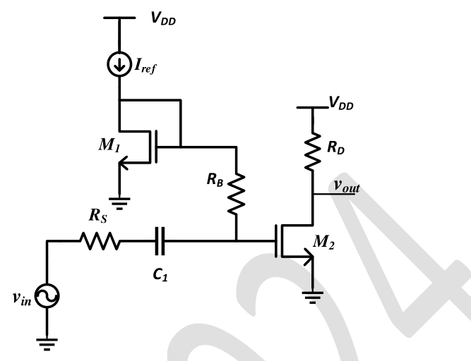
In the circuit shown below, the transistors $M_1$ and $M_2$ are biased in saturation. Their small signal transconductances are $g_{m1}$ and $g_{m2}$, respectively. Neglect body effect, channel length modulation and intrinsic device capacitances.
Assuming that capacitor $C_1$ is a short circuit for AC analysis, the exact magnitude of small signal voltage gain $\left|\dfrac{v_{out}}{v_{in}}\right|$ is ______.
Practise this question in The GATE Grind →
Show answer and explanation
Correct answer: (B) $\dfrac{g_{m2}R_D\left(R_B+\frac1{g_{m1}}\right)}{R_B+\frac1{g_{m1}}+R_S}$
Explanation
$I_{ref}$ is an ideal current source (open for AC), so the diode-connected $M_1$ looks like $1/g_{m1}$ to ground. The gate of $M_2$ therefore sees $R_S$ in series with $R_B+1/g_{m1}$ to ground, and no DC path draws signal current. $v_{g2}=v_{in}\dfrac{R_B+1/g_{m1}}{R_S+R_B+1/g_{m1}}$. $M_2$ gives $v_{out}=-g_{m2}R_Dv_{g2}$, so $|v_{out}/v_{in}|=\dfrac{g_{m2}R_D(R_B+1/g_{m1})}{R_B+1/g_{m1}+R_S}$.