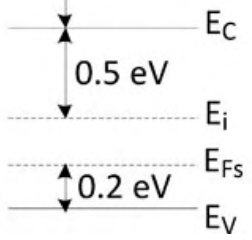
The band diagram of a $p$-type semiconductor with a band-gap of 1 eV is shown. Using this semiconductor, a MOS capacitor having $V_{TH}$ of $-0.16$ V, $C'_{ox}$ of 100 nF/cm$^2$ and a metal work function of 3.87 eV is fabricated. There is no charge within the oxide. If the voltage across the capacitor is $V_{TH}$, the magnitude of depletion charge per unit area (in C/cm$^2$) is
The vacuum level is 4 eV above $E_C$, and the Fermi level is 0.2 eV above $E_V$ (0.8 eV below $E_C$), so the semiconductor work function is $4+0.8=4.8$ eV. Then $\phi_{ms}=3.87-4.8=-0.93$ V. The Fermi potential is $\phi_F=E_i-E_{Fs}=0.5-0.2=0.3$ V, so $2\phi_F=0.6$ V. From $V_T=\phi_{ms}+2\phi_F+\frac{|Q_d|}{C_{ox}}$: $|Q_d|=100\text{ nF/cm}^2\times(-0.16+0.93-0.6)=1.70\times10^{-8}$ C/cm$^2$.
More P-N Junction and Semiconductor Devices questions
GATE 2020 EC Q43– The base of an npn BJT T1 has a linear doping profile N B(x) as shown below. The base of…
GATE 2020 EC Q44– A pn junction solar cell of area 1.0 cm2, illuminated uniformly with 100 mW cm-2, has the…
GATE 2019 EC Q20– The figure shows the high-frequency C-V curve of a MOS capacitor (at T = 300 K) with ms=0…
GATE 2019 EC Q45– The quantum efficiency () and responsivity (R) at a wavelength (in m) in a p-i-n…
GATE 2019 EC Q59– In an ideal pn junction with an ideality factor of 1 at T=300 K, the magnitude of the…
GATE 2018 EC Q17– In a p-n junction diode at equilibrium, which one of the following statements is NOT TRUE?