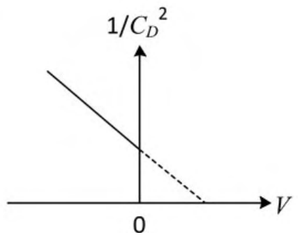
A one-sided abrupt $pn$ junction diode has a depletion capacitance $C_D$ of 50 pF at a reverse bias of 0.2 V. The plot of $1/C_D^2$ versus the applied voltage $V$ for this diode is a straight line as shown in the figure below. The slope of the plot is ________ $\times10^{20}\ \text{F}^{-2}\text{V}^{-1}$.
For an abrupt one-sided junction, $\frac{1}{C_D^2}=\frac{2(\phi_{bi}-V)}{q\varepsilon N A^2}$, so the slope is $-\frac{1}{C_D^2(\phi_{bi}+V_R)}$ at any reverse bias $V_R$. At $V_R=0.2$ V, $\frac{1}{C_D^2}=\frac{1}{(50\text{ pF})^2}=4\times10^{20}$, and with $\phi_{bi}\approx0.5$ V the slope is $-\frac{4\times10^{20}}{0.7}\approx-5.7\times10^{20}\ \text{F}^{-2}\text{V}^{-1}$.
More P-N Junction and Semiconductor Devices questions
GATE 2020 EC Q42– The band diagram of a p-type semiconductor with a band-gap of 1 eV is shown. Using this…
GATE 2020 EC Q43– The base of an npn BJT T1 has a linear doping profile N B(x) as shown below. The base of…
GATE 2020 EC Q44– A pn junction solar cell of area 1.0 cm2, illuminated uniformly with 100 mW cm-2, has the…
GATE 2019 EC Q20– The figure shows the high-frequency C-V curve of a MOS capacitor (at T = 300 K) with ms=0…
GATE 2019 EC Q45– The quantum efficiency () and responsivity (R) at a wavelength (in m) in a p-i-n…
GATE 2019 EC Q59– In an ideal pn junction with an ideality factor of 1 at T=300 K, the magnitude of the…