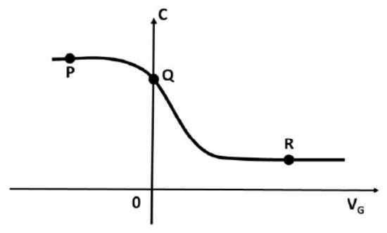
The figure shows the high-frequency C-V curve of a MOS capacitor (at T = 300 K) with $\Phi_{ms}=0$ V and no oxide charges. The flat-band, inversion, and accumulation conditions are represented, respectively, by the points
For a $p$-type substrate, a negative gate voltage gives accumulation (high capacitance, point P), $V_G=0$ is the flat-band condition (point Q, since $\Phi_{ms}=0$ and there are no oxide charges) and large positive $V_G$ gives inversion with the low high-frequency capacitance (point R). So the order is Q, R, P.
More P-N Junction and Semiconductor Devices questions
GATE 2019 EC Q45– The quantum efficiency () and responsivity (R) at a wavelength (in m) in a p-i-n…
GATE 2019 EC Q59– In an ideal pn junction with an ideality factor of 1 at T=300 K, the magnitude of the…
GATE 2018 EC Q17– In a p-n junction diode at equilibrium, which one of the following statements is NOT TRUE?
GATE 2018 EC Q28– A p-n step junction diode with a contact potential of 0.65 V has a depletion width of 1 m…
GATE 2018 EC Q30– There are two photolithography systems: one with light source of wavelength 1=156 nm…
GATE 2018 EC Q40– Red (R), Green (G) and Blue (B) Light Emitting Diodes (LEDs) were fabricated using p-n…