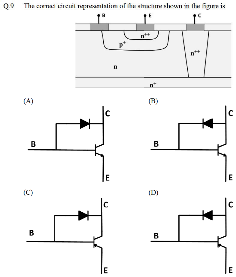
The structure is an $npn$ transistor whose base ($p^+$) contact is also connected to the collector ($n$ epitaxial layer through $n^{++}$), which forms a diode from base (anode) to collector (cathode). Circuit (A) shows the diode with its anode at the base and cathode at the collector.
More BJT and MOSFET Amplifiers questions
GATE 2019 EC Q50– In the circuits shown, the threshold voltage of each nMOS transistor is 0.6 V. Ignoring…
GATE 2019 EC Q60– Consider a long-channel MOSFET with a channel length 1\ m and width 10\ m. The device…
GATE 2019 EC Q64– In the circuit shown, the threshold voltages of the pMOS ( V tp ) and nMOS (V tn)…
GATE 2019 EC Q65– In the circuit shown, V 1=0 and V 2=V dd. The other relevant parameters are mentioned in…
GATE 2018 EC Q11– Two identical nMOS transistors M 1 and M 2 are connected as shown below. The circuit is…
GATE 2018 EC Q53– In the circuit shown below, the (W/L) value for M 2 is twice that for M 1. The two nMOS…