GATE 2019 EC – Question 50
In the circuits shown, the threshold voltage of each nMOS transistor is 0.6 V. Ignoring the effect of channel length modulation and body bias, the values of $V_{out1}$ and $V_{out2}$, respectively, in volts, are
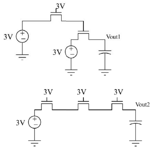
Practise this question in The GATE Grind →
Show answer and explanation
Correct answer: (C) 1.8 and 2.4
Explanation
In the first circuit the top nMOS (gate at 3 V, source input 3 V) passes at most $3-0.6=2.4$ V. The second nMOS has its gate tied to its drain (at 2.4 V), so its output can rise only to $2.4-0.6=1.8$ V, giving $V_{out1}=1.8$ V. In the second circuit all three pass transistors have their gates at 3 V and pass the 3 V input up to $3-0.6=2.4$ V, so $V_{out2}=2.4$ V.