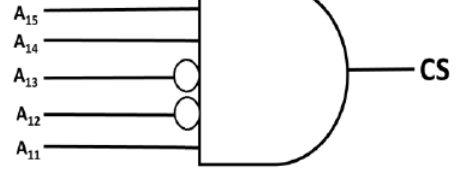
The chip select logic for a certain DRAM chip in a memory system design is shown below. Assume that the memory system has 16 address lines denoted by $A_{15}$ to $A_0$. What is the range of addresses (in hexadecimal) of the memory system that can enable the chip select (CS) signal?
The AND gate has inverted inputs on $A_{13}$ and $A_{12}$, so CS is active for $A_{15}A_{14}A_{13}A_{12}A_{11}=11001$. The remaining 11 address lines run from all 0s to all 1s, giving $1100\ 1000\ 0000\ 0000=$ C800 to $1100\ 1111\ 1111\ 1111=$ CFFF.
More Memory Interfacing and Hierarchy questions
GATE 2019 CS Q43– Assume that in a certain computer, the virtual addresses are 64 bits long and the physical…
GATE 2019 CS Q55– A certain processor deploys a single-level cache. The cache block size is 8 words and the…
GATE 2018 CS Q33– A 32-bit wide main memory unit with a capacity of 1 GB is built using 256M 4-bit DRAM…
GATE 2018 CS Q44– The size of the physical address space of a processor is 2P bytes. The word length is 2W…
GATE 2016 CS (CS1) Q19– A processor can support a maximum memory of 4 GB, where the memory is word-addressable (a…
GATE 2017 CS (CS1) Q35– Consider a two-level cache hierarchy with L1 and L2 caches. An application incurs 1.4…