GATE 2023 EC – Question 19
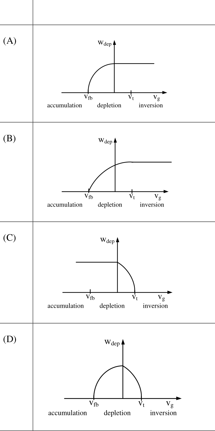
For a MOS capacitor, $V_{fb}$ and $V_t$ are the flat-band voltage and the threshold voltage, respectively. The variation of the depletion width ($W_{dep}$) for varying gate voltage ($V_g$) is best represented by
Practise this question in The GATE Grind →
Show answer and explanation
Correct answer: (B) Plot (B)
Explanation
For $V_g<V_{fb}$ the device is in accumulation and there is no depletion region ($W_{dep}=0$). Between $V_{fb}$ and $V_t$ (depletion) $W_{dep}$ grows with $V_g$. Beyond $V_t$ (inversion) the inversion layer screens the gate charge and $W_{dep}$ stays at its maximum value. The curve therefore rises from $V_{fb}$ and becomes flat exactly at $V_t$, which is plot (B).