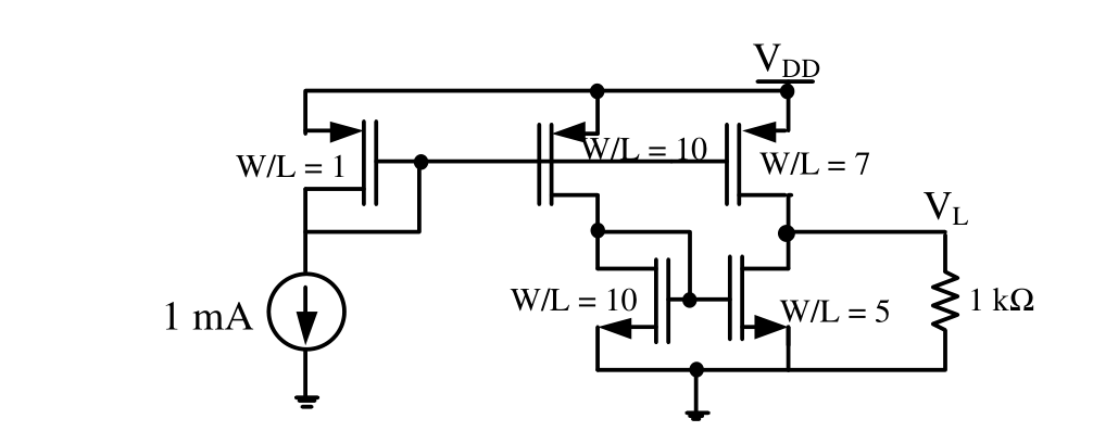
The 1 mA reference flows in the diode-connected PMOS with $W/L=1$. The PMOS with $W/L=10$ mirrors 10 mA, and the PMOS with $W/L=7$ mirrors 7 mA. The 10 mA feeds the diode-connected NMOS ($W/L=10$), and the NMOS with $W/L=5$ mirrors half of that: 5 mA. At node $V_L$, 7 mA is supplied from the top and 5 mA is pulled down by the NMOS, so the net 2 mA flows through the 1 kΩ resistor: $V_L=2\text{ mA}\times1\text{ k}\Omega=2.00$ V (all transistors assumed in saturation).
More BJT and MOSFET Amplifiers questions
GATE 2022 EC Q18– Consider the CMOS circuit shown in the figure (substrates are connected to their…
GATE 2022 EC Q20– The ideal long channel nMOSFET and pMOSFET devices shown in the circuits have threshold…
GATE 2022 EC Q40– Consider an ideal long channel nMOSFET (enhancement-mode) with gate length 10\ m and width…
GATE 2022 EC Q59– Consider the circuit shown with an ideal long channel nMOSFET (enhancement-mode, substrate…
GATE 2021 EC Q18– In the circuit shown in the figure, the transistors M 1 and M 2 are operating in…
GATE 2021 EC Q54– For the transistor M 1 in the circuit shown in the figure, nC ox=100\ A/V2 and (W/L)=10,…