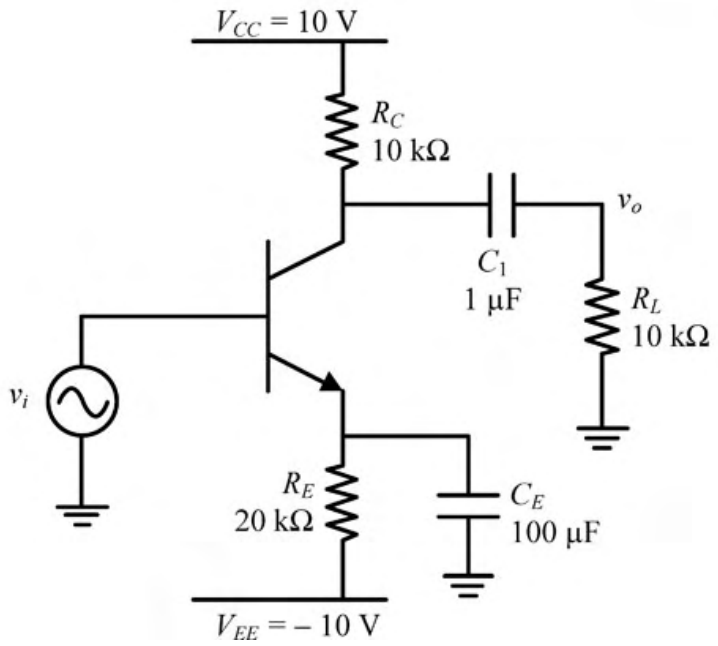
For the BJT in the amplifier shown below, $V_{BE}=0.7$ V, $kT/q=26$ mV. Assume that BJT output resistance ($r_o$) is very high and the base current is negligible. The capacitors are also assumed to be short circuited at signal frequencies. The input $V_i$ is direct coupled. The low frequency voltage gain $v_o/v_i$ of the amplifier is
DC bias: the base is at 0 V, so $I_E=\frac{0-0.7-(-10)}{20\text{ k}\Omega}=0.465$ mA and $I_C\approx0.465$ mA. Then $g_m=\frac{I_C}{V_T}=\frac{0.465\text{ mA}}{26\text{ mV}}=17.9$ mS. The emitter is bypassed by $C_E$, so the gain is $-g_m(R_C\|R_L)=-17.9\text{ mS}\times5\text{ k}\Omega=-89.4$.
More BJT and MOSFET Amplifiers questions
GATE 2020 EC Q46– An enhancement MOSFET of threshold voltage 3 V is being used in the sample and hold…
GATE 2020 EC Q47– Using the incremental low frequency small-signal model of the MOS device, the Norton…
GATE 2020 EC Q54– In the voltage regulator shown below, V I is the unregulated input at 15 V. Assume V…
GATE 2019 EC Q19– The correct circuit representation of the structure shown in the figure is
GATE 2019 EC Q50– In the circuits shown, the threshold voltage of each nMOS transistor is 0.6 V. Ignoring…
GATE 2019 EC Q60– Consider a long-channel MOSFET with a channel length 1\ m and width 10\ m. The device…