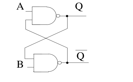
For the circuit shown below, the propagation delay of each NAND gate is 1 ns. The critical path delay, in ns, is ________ (rounded off to the nearest integer).
The circuit is a cross-coupled NAND SR latch. A change at an input must pass through the first NAND to change $Q$, and then through the second NAND (through the feedback) to update $\bar Q$. The longest path has two gates, so the critical path delay is $2\times1$ ns $=2$ ns.
More Sequential Circuits questions
GATE 2023 EC Q63– In a given sequential circuit, initial states are Q 1=1 and Q 2=0. For a clock frequency…
GATE 2022 EC Q43– For the circuit shown, the clock frequency is f 0 and the duty cycle is 25%. For the…
GATE 2021 EC Q56– The propagation delay of the exclusive-OR (XOR) gate in the circuit in the figure is 3 ns.…
GATE 2020 EC Q49– The state diagram of a sequence detector is shown below. State S 0 is the initial state of…
GATE 2020 EC Q60– For the components in the sequential circuit shown below, t pd is the propagation delay, t…
GATE 2019 EC Q35– In the circuit shown, the clock frequency, i.e., the frequency of the Clk signal, is 12…